


Please Leave Us A Message
Privacy statement: Your privacy is very important to Us. Our company promises not to disclose your personal information to any external company with out your explicit permission.
 January 10, 2022
For example, the EU CoC V5 TIer 2, which came into effect on January 1, 2016, requires an average energy efficiency of 87.7% and 89% for AC-DC adapters with output power of 45 W and 65 W, respectively, and standby power consumption of less than 75 mW and 150 mW, and also required energy efficiency of 10% load conditions to reach 77.7% and 77.5%. Power design engineers face design challenges in terms of size, energy efficiency, and cost.
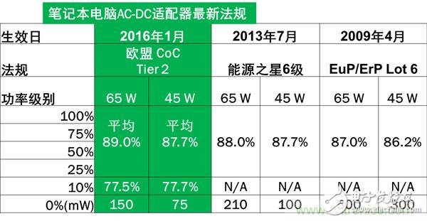
Table 1. List of AC-DC Adapter Energy Efficiency Regulations
The switching frequency directly determines the power density of the switching power supply. Increasing the switching frequency can effectively reduce the size of passive power devices such as transformers and output capacitors, thereby increasing power density; high power density applications are only insufficient to meet energy efficiency specifications because of volume reduction. In an hour, the heat dissipation area is also reduced accordingly. Energy efficiency is required to reduce heat generation and reduce the impact on the life of internal components. In addition, engineers need to control the cost within a reasonable range to be in a favorable position in a highly competitive market.
Quasi-resonant flyback + synchronous rectification = high power density adapter
The LLC topology provides high frequency and energy efficiency, but it is costly and has a strict input voltage range and is not suitable for notebook power levels. High-power density adapters that meet volume, energy efficiency, cost, etc., such as ON Semiconductor's high-frequency quasi-resonant flyback controller NCP1340/1, can be easily designed using a quasi-resonant flyback topology plus synchronous rectification (SR) +SR Control IC NCP4305/80.
The quasi-resonant mode allows the use of a relatively large snubber capacitor, Clump, and an additional Clump (10-22pF) reduces MOSFET turn-off losses and reduces electromagnetic interference (EMI). The quasi-resonant flyback is beneficial to the sub-extreme plus SR, which can reduce the conduction loss of the rectifier diode, reduce the peak voltage of the secondary rectifier and reduce its withstand voltage requirement.
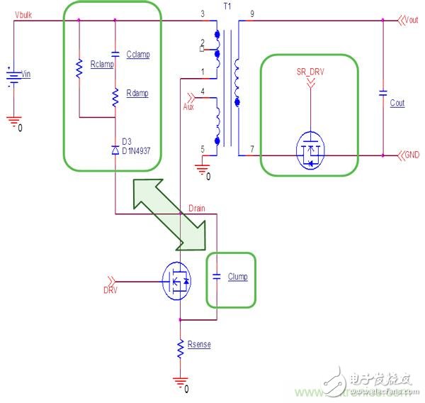
Figure 1. Quasi-resonant mode allows the use of a relatively large snubber capacitor Clump
Quasi-resonant flyback power loss analysis and design points
Analysis of quasi-resonant flyback losses is designed to increase the operating frequency and then reduce power losses. The losses of the quasi-resonant flyback power supply are mainly distributed in the primary MOSFET, the peak snubber circuit, the transformer, and the output rectification.
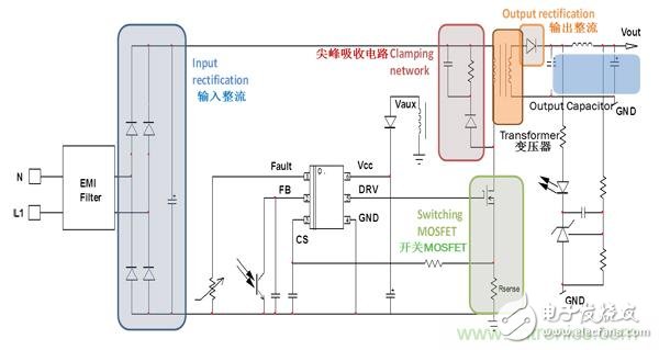
Figure 2. Loss distribution of a quasi-resonant flyback power supply
1. Primary MOSFET loss analysis
Primary MOSFET losses mainly include conduction loss, switching loss, and drive loss. The conduction loss is defined by the drain-source on-resistance Rds(on) and the primary-side rms current. For switching losses, since the junction capacitance of the MOSFET is nonlinearly proportional to its Vds voltage, it cannot be calculated by a simple capacitor energy storage formula. The actual junction capacitance needs to be taken into account. The junction capacitance can be understood as the equivalent of the MOSFET DS network. Other capacitors outside the junction capacitance of the MOSFET. The drive loss can be ignored when the switching frequency is low, but it cannot be ignored in high frequency applications. It is generated when the MOSFET is turned on and off, mainly depending on the total gate charge Qg of the MOSFET, the switching frequency, and the IC operating voltage Vcc. Most of the losses are consumed on the drive resistors.
Therefore, for the selection of MOSFETs, in high frequency applications, the lower the number of Rds (on) x Qg products, the better the conduction loss and drive loss are reduced. A low thermal resistance package with small size, thinness, and good heat dissipation should be selected. Since gallium nitride (GaN) MOSFETs have better Rds (on) x Qg parameters, an additional 0.3% full load efficiency can be added, and GaN MOSFETs are an ideal choice when cost permits.
2. Peak absorption circuit loss analysis
The spike absorption circuit is mainly used to clamp the Vds voltage of the MOS transistor to prevent its overvoltage breakdown. Resistor-capacitor-diode (RCD) absorption and transient voltage suppressor (TVS) absorption are two commonly used circuits, of which RCD is the most commonly used and has high reliability.
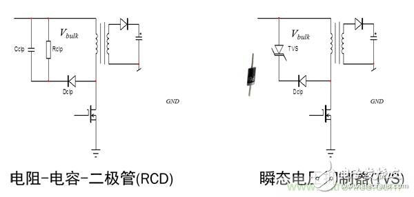
Figure 3. Two common spike absorption circuits
For the RCD circuit, the larger snubber capacitor C can reduce the clamp voltage ripple, but it will increase the standby power consumption. Therefore, the selection of C is generally 5% to 10% clamp voltage ripple at full load. If the absorption resistance R is hot, the leakage inductance of the transformer can be reduced. The slow tube with good Trr consistency can be used to reduce the clamping voltage and reduce the R loss.
In terms of clamping voltage, selecting a high clamping voltage can reduce the RCD absorption loss, but it is necessary to select a high withstand voltage MOS tube, which will lead to an increase in cost, and the primary current decay rate of the transformer will become faster, and the slope of the secondary rectified current will become steeper. It is not conducive to EMI and secondary synchronous rectification efficiency optimization. Choosing a low clamping voltage facilitates EMI, secondary synchronous rectification control, but RCD absorption losses increase. The rectifier diode D uses a slow tube to reduce the clamping voltage and improve EMI, but the diode temperature rise will be higher. Therefore, we need to consider all aspects of the impact and weigh the options.
3. Transformer loss analysis
The above is the High-frequency quasi-resonant flyback reference design for ultra-high power density compact adapters we have listed for you. You can submit the following form to obtain more industry information we provide for you.
You can visit our website or contact us, and we will provide the latest consultation and solutions
Send Inquiry
Most Popular
lastest New
Send Inquiry
Send Inquiry

Mr. luokailiang
Tel:86--13590295313
Fax:
Mobile Phone:+8613590295313
Email:369488374@qq.com
Address:201A,2nd Floor,Building5,Xinjihui Industrial Zone,Xinxue Community,Bantian Street,Longgang District, Shenzhen, Guangdong
Related Products List
Mobile Site
Privacy statement: Your privacy is very important to Us. Our company promises not to disclose your personal information to any external company with out your explicit permission.
Fill in more information so that we can get in touch with you faster
Privacy statement: Your privacy is very important to Us. Our company promises not to disclose your personal information to any external company with out your explicit permission.